back
 BootROM Replacement
The mass production SEGA Dreamcast has a built-in 2 MByte BootROM which cannot be re-programmed.
In addition to that it also has a built-in 256 KByte FlashROM, but one of the address lines is
not connected, so only 128 KByte are available. When the box is powered on, the SH4 CPU starts
executing code from address 0xA0000000, which happens to be the built-in 2 MByte BootROM.
Replacing the original BootROM can be useful especially during development work on the box to reduce
the boot time after a system reset. The replacement FlashROM chip must be a 3.3 V CMOS one. However,
the packaging of today's chips can be somewhat challenging to solder with a normal soldering iron.
I have successfully used a Spansion S29AL004D 512K x 8 FlashROM packaged as TSOP-48 for the actual
FlashROM. Additionally an IDTQS3257 CMOS Quad 2:1 MUX/DEMUX is used to implement the switching between
the original built-in BootROM and the replacement FlashROM.
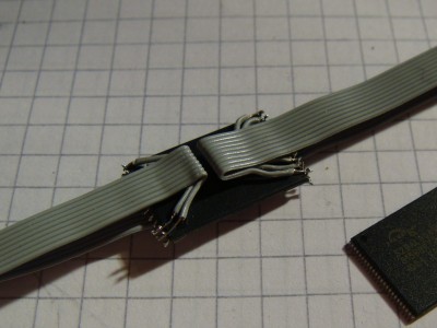
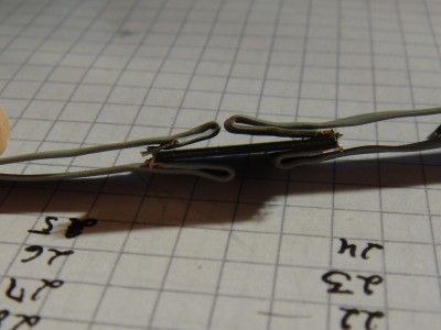
In order to be able to solder wires to the TSOP-48 chip more comfortably, its pins can be bent alternatively
up and down as shown on the picture below. Wires will then be attached at the top and at the bottom of the chip.
This gives more space between the pins and simplifies soldering a lot. Removing pins that will not be connected also helps.

Attaching the wires requires a steady hand a bit of patience :)
The most annoying thing here is that the soldering surface (the pins and the wires) are small and tend to break off
if the wires are moved too much.


Finding a good place for the FlashROM is not so difficult. The original mainboard shielding metal sandwich construction
leaves room for stuff that can be placed on top of the board. Alternatively it could also be placed at the other side of
the board, where there are a lot of soldering pads available for almost all the signals. I did it as shown below, by attaching
the wires of the FlashROM to the pins of the original BootROM.

The original BootROM does not have a WE# signal, since it is a read-only memory chip. The required WE# signal for the sandwiched FlashROM
can be taken from either the built-in FlashROM or the GD-ROM connector CN503. This is because the built-in BootROM, built-in FlashROM and
the GD-ROM drive are all connected to the G1 bus in parallel. Also the CE# pin of the original BootROM (IC501) has to be disconnected from the
PCB, so that a switch can be connected to select between the BootROM or the sandwiched FlashROM. The switch will basically connect either
the original BootROM's CE# pin or the sandwiched FlashROM's CE# pin to the CE# line on the PCB. If the CE# pin of either one of the chips is
disconnected from the board it must be pulled up to Vcc. This can be implemented with a 2:1 MUX/DEMUX.

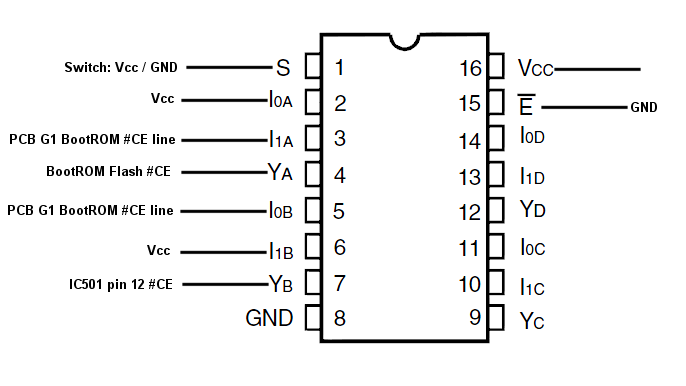
Below is the wiring of the IDTQS3257 CMOS Quad 2:1 MUX/DEMUX. Vcc is 3.3V which is fairly easy to get anywhere on the board.
The S input should be either connected to Vcc or GND. This can be accomplished easily with a 3 pin pyhsical switch.
To get away with a 2 pin switch a simple pull-up or pull-down circuit can be used.

 BootROM Replacement
